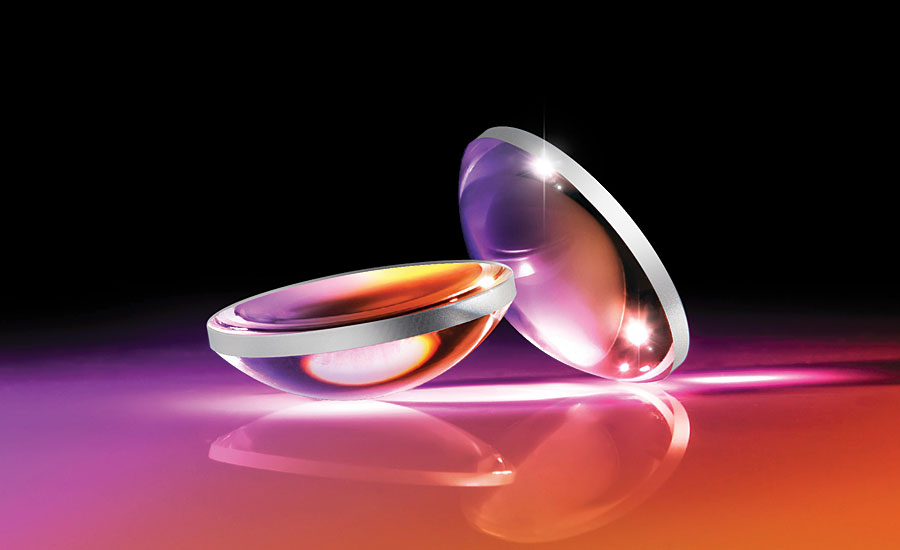
Optical applications and devices are seen in every aspect of humans’ lives. Real-time applications of objects can be seen in a technologies and day-to-day objects such as mirrors, convex & concave lenses, contact lenses, telescopes, microscopes, Lasers, and fiber optics. Not to mention, fiber optics has revolutionized the telecommunications industry and internet communications. All in all, there is a plethora of benefits to the developments of optic technology such as entertainment, medicine (surgery, in particular), and defence.
In the beginning, the term ‘Optics’ was applied only in relation to eyes, essentially vision. Later, devices that helped vision such as lenses were developed, and were called optical instruments. Development of lenses by ancient Egyptians and Mesopotamians, theories of light & vision by ancient Greek philosophers, and the development of geometrical optics in the Greek-Roman world were the reasons behind the onset of Optics. These primitive studies on optics were referred to as ‘Classical Optics’ while the areas of optical research that substantially developed in the 20th century is referred to as ‘Modern Optics’. Classical optics is categorized into two main branches – geometrical optics (also known as Ray optics) and physical optics (wave optics).
Optics in Manufacturing
The manufacturing is being transformed by the application of Optics that has the capability to improve the contemporary manufacturing potential make way for new ones. Using light, we can process materials remotely, even through windows separating harsh or vacuum environments.
Owing to the various distinct properties of light and the interaction between light & matter, light offers numerous varieties of applications in the manufacturing processes. Light has two great benefits – excellent imaging properties and the ability to induce photochemical reactions that permit highly complicated mask patterns to be transported to photoresist in the optical lithography process.

Photolithography
Photolithography, aka optical lithography or UV lithography, plays a key role in integrated circuit processing. Using light, it transfers a geometrical pattern from a photomask to a photosensitive chemical photoresist on upon the substrate. Following this, a sequence of chemical treatments etches the exposed pattern into the material or facilitates the disposition of a new material in the expected pattern.
Because of the demand for higher processing speeds, there is increased pressure on photographic processes, new Photolithographic tools, newest materials, light sources of shorter wavelengths, and advanced optical system designs alike. The workhorse of photolithographic processes is the Step-and-Repeat camera. The substitutes for future advances in ‘Photolithography’ are numerous. A few of them include wavefront engineering, Extreme Ultraviolet (EUV), and electron beam.


